Table Of Content
In this tutorial, we'll show all the steps involved in creating your circuits and schematics, then we'll transition into creating a circuit board design that can actually be manufactured. Printed circuit boards came from electrical connection systems that were used in the 1850s. Originally metal strips or rods were used to connect large electric components mounted on wooden bases.
The Process of Printed Circuit Board Design
The silkscreen adds letters, numbers, and symbols to the PCB that allow for easier assembly and indicators for humans to better understand the board. We often use silkscreen labels to indicate what the function of each pin or LED. In the example below, the green solder mask is applied to the majority of the PCB, covering up the small traces but leaving the silver rings and SMD pads exposed so they can be soldered to. Because the software will compare what you are drawing to the schematics file. Class 2 boards are found in devices where high reliability is important, but not crucial. Producing vPCBs wouldn't entail major changes to manufacturing processes.

Create the Schematic
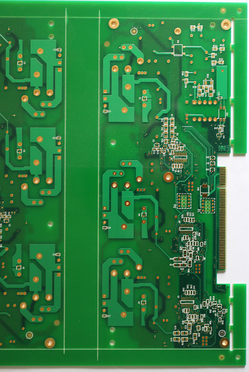
A printed circuit board, or PCB, is a board made of an insulating material that contains conductive pathways etched onto its surface. The conductive pathways are typically made of copper, and are used to connect different electronic components together in a circuit. The process of designing and manufacturing PCBs involves specialized software and equipment, and is an important part of the electronics industry.In this article, we will do a deep dive on printed circuit boards. We’ll learn what PCBs are, how they are constructed, manufactured, designed, and even reverse-engineered. Printed circuit boards (PCBs) are the foundation of modern electronics, providing a reliable method of connecting electronic components.
Extended Data Fig. 1 Dynamic mechanical analysis of pristine and recycled vitrimer.
Common layer configurations include power and ground planes, signal layers, and dedicated layers for specific purposes like shielding or heat dissipation. The bare PCB is made up of land patterns for components to be attached/soldered on to the PCB. They are interconnected by a conductive printed wire referred to as a trace on a non-conductive substrate.
Source Data Fig. 3
These rules can be applied to individual objects or to groups of objects using queries or using Net Class objects. Take a look at this article to see how you can set up a Net Class in Altium Designer. When you transfer your schematic information to the PcbDoc the component footprints are shown in addition the board outline specified. Prior to placing components you should define the PCB layout (i.e. shape, layer stackup) using the Layer Stackup Manager, shown below.
You’ll have the best PCB design technology on the market when you use Altium Designer. The surface of a printed circuit board is where the components and conductive traces are located. Double-sided PCBs have components and traces on both sides of the board, connected by through-hole vias or surface-mounted vias.The surface of a PCB can also be covered with a layer of solder mask. Solder mask is a protective coating that helps to prevent shorts and other types of damage to the board.
RIT partners with industry experts on new curriculum in electronics design and manufacturing RIT - Rochester Institute of Technology
RIT partners with industry experts on new curriculum in electronics design and manufacturing RIT.
Posted: Tue, 15 Feb 2022 08:00:00 GMT [source]

When selecting metal core materials for a PCB, it is essential to consider the application's specific requirements, such as thermal performance, weight, and cost. It’s important to note that reverse engineering a PCB can be a complex and time-consuming process, and it may be difficult to create an exact replica of the original. Additionally, reverse engineering may not be legal in all situations, so it’s important to verify the legality of reverse engineering any specific piece of technology before attempting this process. The choice of PCB type depends on the specific requirements of the application, including the complexity of the circuit, the available space, and the desired performance characteristics.
Biodegradable elastomeric circuit boards from citric acid-based polyesters
You can define these groups in the PCB layout, or you can define groups on the schematic using Cross Select Mode, which is accessible from the Tools menu. When designing a printed circuit board (PCB), one of the critical factors to consider is the return current path. The return current path refers to the path that the current takes to complete the circuit and return to its source. A clear and well-defined return current path is essential for the proper functioning of the PCB and to avoid any potential issues.
Routing refers to the process of creating connections between different components on the PCB, ensuring that the electrical signals flow smoothly and efficiently. It determines the overall performance, reliability, and manufacturability of the circuit board. Proper PCB routing helps to minimize signal interference, reduce noise, and optimize the flow of electrical signals. It also ensures that the PCB meets the required electrical and mechanical specifications. Before you start routing, it is essential to have a clear plan for your PCB layout. Consider the placement of components, the size of the board, and any specific design requirements.
Surface-mount technology, on the other hand, is used for smaller, sensitive components like resistors, diodes and the like. Because they are mounted straight to the board, as opposed to through it, the use of smaller components frees up portions of the board that might otherwise have been taken up by leads and solder from larger components. When a component is mounted using a through-hole, the component is actually plugged in through holes in the board itself, with the component’s leads punched through the PCB to the other side.
Multiple etched layers are laminated in succession until the printed circuit board stack-up is complete. This is the overall process used in PCB design fabrication, where the bare board is formed before passing through a printed circuit board's assembly process. Printed circuit board (PCB) design has grown into its own specialized field within the electronics industry.
Understanding the basic concepts and terminology related to PCB design is essential for creating reliable and efficient electronic products. If you want to easily get through all of these stages in the PCB electronics board design process, you need to use the best design software with an intuitive user interface and a complete set of PCB design features. The next generation of PCB design and fabrication marks a convergence with component packaging, which is used to hold semiconductor chips in ICs. Chips in advanced processors and digital/RF modules are placed on an IC substrate, which provides the interconnections between the electrical contacts on the semiconductor die and the PCB. The most advanced ICs are implementing feature sizes that are similar to features found in IC substrates, and the same manufacturing processes are used to produce both IC substrates and UHDI PCBs. The right printed-circuit-board (PCB) design can make or break a project, which is why it’s important to have the proper materials and expertise from the get-go.
These files contain all the necessary information for producing the circuit board, including the component placement, routing, and drill holes. The files are then sent to a manufacturer like NextPCB, who produces the PCB according to the specifications. The Board Class is a classification system used to categorize the quality and reliability of a printed circuit board.


No comments:
Post a Comment